ESP32-S3 RF Development Board
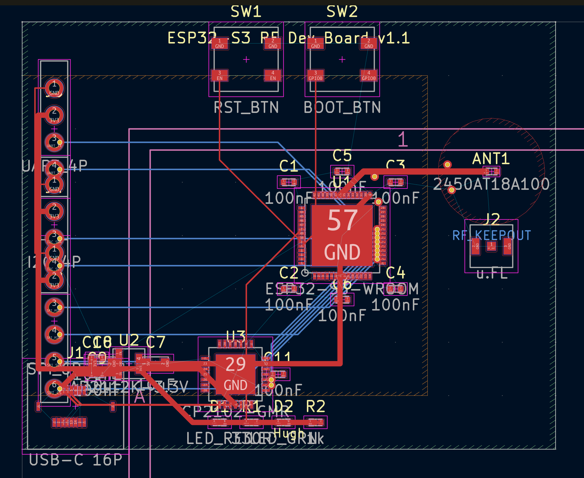
4-layer RF dev board around the bare ESP32-S3FN8 QFN56 die (not a module), KiCAD 8, 50 x 40 mm, JLC04161H-7628 stackup. Files generated programmatically via generate_board.py.
Components
| Ref | Part | Notes |
|---|---|---|
| U1 | ESP32-S3FN8 QFN56 | Dual-core LX7, 8 MB internal flash, 2.4 GHz WiFi/BT5 |
| U2 | AP2112K-3.3V | 600 mA LDO |
| U3 | CP2102-GMR | USB-UART |
| U4 | USBLC6-2SC6 | USB D+/D- ESD clamp |
| Y1 | NX3225GA 40.000 MHz | 10 ppm main clock |
| ANT1 | Johanson 2450AT18A100 | 2.4 GHz chip antenna |
| J2 | u.FL SMD | RF test port (S11 / VNA) |
| TP1-3 | 1.5 mm SMD pads | 3V3, GND, RF_ANT probe points |
Stackup
| Layer | Function |
|---|---|
| L1 F.Cu | Signals, RF trace |
| Prepreg | 0.2 mm, Er = 4.4 |
| L2 In1.Cu | Solid GND |
| Core | FR4, 1.065 mm |
| L3 In2.Cu | 3.3V plane |
| L4 B.Cu | Secondary signals |
RF Design
RF trace from ESP32-S3 RF pin to ANT1: 50 ohm microstrip, 0.6 mm width (IPC-2141A, h=0.2 mm, Er=4.4). All bends 45 degrees.
Antenna keepout: 5 mm radius on F.Cu, In1.Cu, B.Cu. In1.Cu cutout is the critical one; a GND plane under the antenna collapses radiation resistance.
GND stitching vias along the RF trace at 6 mm spacing (lambda/10 at 2.4 GHz in FR4).
J2 (u.FL) shares the RF_ANT net with ANT1. A 0-ohm series jumper selects between chip antenna and VNA port for bring-up S11 measurement.
Clock and Boot
40 MHz NX3225GA crystal with 2x 12 pF NP0 load caps (C12, C13) on XTAL_P / XTAL_N. ESP32-S3FN8 has 8 MB of internal SPI flash, so no external flash IC is needed. R5 (10k) pulls EN to 3V3 so the reset button has a pull against.
USB-C
- R3, R4: 5.1k CC1/CC2 pull-downs for device negotiation
- U4: USBLC6-2SC6 ESD clamp on D+/D-
- R6, R7: 22R series damping on D+/D- between U4 and CP2102
Power
AP2112K-3.3V, USB 5V in. ESP32-S3 peaks ~350 mA during WiFi TX (600 mA rated, ~250 mA margin). 10 uF bulk caps on LDO in/out; 100 nF decoupling within 2 mm of every VCC pin.
Programmatic Generation
The PCB, schematic, and BOM are generated from Python rather than hand-drawn. generate_board.py emits .kicad_pcb, .kicad_sch, .kicad_pro, and bom.csv; reroute_clean.py re-routes after position changes; fix_pcb.py patches UUIDs and zone-fill syntax. Design parameters (trace widths, keepout radii, component positions) live in code and are version-controlled.
DRC progress
| Stage | Violations | Unconnected |
|---|---|---|
| Pre-v1.2 baseline | 447 | 70 |
| After sch + crystal + flash fixes | 144 | 122 |
| After programmatic DRC cleanup | 33 | 120 |
Remaining 33 are cosmetic (courtyard overlaps, silk-over-copper, dangling vias). The 120 unconnected nets are power/USB/UART/I2C/SPI fanout pending a Pcbnew routing pass before Gerber export.
Bring-up Firmware
ESP-IDF v5. WiFi scan every 10 seconds over UART at 115200 to verify the RF path. GPIO48 status LED at 1 Hz. Source in firmware/.